Eva Olsson Group | Chalmers
  • HOME
  • NEWS & EVENTS
  • RESEARCH
  • MEMBERS
  • OPENINGS
  • CONTACT
  • PHOTOGRAPHS
  • HOME
  • NEWS & EVENTS
  • RESEARCH
  • MEMBERS
  • OPENINGS
  • CONTACT
  • PHOTOGRAPHS
Search
Picture

Picture
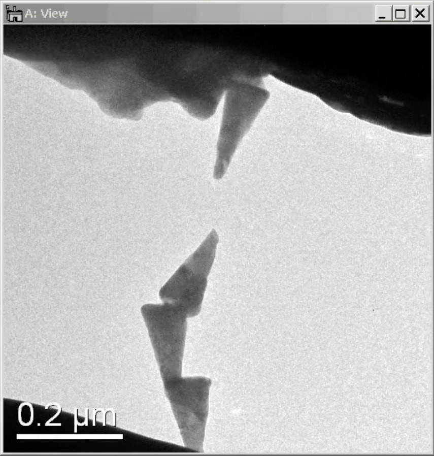
In Situ TEM movie showing manipulation and biasing of Au nanocones.
Dr. Ludvig de Knoop 
Biography
Ludvig earned his degree of Master of Science in Engineering Physics at Chalmers University of Technology in 2005. During his master thesis project, supervised by Eva Olsson and Krister Svensson, he studied electron transport measurements in carbon nanotubes using in situ TEM biasing. Between 2005 and 2007 he worked as Product Manager for the TEM-NanoIndenter system at Nanofactory Instruments in Gothenburg, Sweden. From 2007 to 2010 he was Vice President of Sales in Europe, Middle East and India for Nanofactory Instruments. In 2014 he earned his PhD in Materials Physics from Université de Toulouse in Toulouse, France, thesis entitled “Development of Quantitative Microscopy for Nanoindentation and Cold-Field Emission” under the supervision of Martin Hÿtch and Marc Legros. He is since 2015 a postdoctoral fellow in the Eva Olsson Group, where he continues working with in situ TEM field emission and other high electric field phenomena.

Research Interests
EM and related techniques:
  • In situ TEM and SEM biasing
  • In situ TEM nanoindentation
  • Electron holography
  • Finite element method modelling
Materials Science:
  • Cold-field emission from gold- and carbon nanocones.
  • Quantification of electric fields using electron holography and simulations.
  • Effects on the atomic structure under intense electric fields, e.g. surface melting (disordering) and field evaporation.
  • Electron bombardment-effects on nano-sized structures.

Publications
  • de Knoop, L., Juhani Kuisma, M., Löfgren, J., Lodewijks, J., Thuvander, M., Erhart, P., Dmitriev, A., Olsson, E., "Electric-field-controlled reversible order-disorder switching of a metal tip surface", Physical Review Materials 2, 085006 (2018). The article can be found here.
  • Holmér, J., Zeng, L., Kanne, T., Krogstrup, P., Nygård, J., de Knoop, L., ​Olsson, E., "An STM – SEM setup for characterizing photon and electron induced effects in single photovoltaic nanowires", Nano Energy 53, pp.175-181 (2018). The article can be found here.
  • Nilsson, H.M., de Knoop, L., Cumings, J., Olsson, E., "Localized resistance measurements of wrinkled reduced graphene oxide using in-situ transmission electron microscopy", Carbon 113(C), pp.340–345 (2017). The article can be found here.
  • Phatak, C., de Knoop, L., Houdellier, F., Gatel, C., Hÿtch, M., Masseboeuf, A., "Quantitative 3D electromagnetic field determination of 1D nanostructures from single projection", Ultramicroscopy 164(C), pp.24–30 (2016). The article can be found here.
  • de Knoop, L., Gatel, C., Houdellier, F., Monthioux, M., Masseboeuf, A., Snoeck, E., Hÿtch, M.J., "Low-noise cold-field emission current obtained between two opposed carbon cone nanotips during in situ transmission electron microscope biasing", Applied Physics Letters 106(26), p.263101 (2015). The article can be found here.
  • Houdellier, F., de Knoop, L., Gatel, C., Masseboeuf, A., Mamishin, S., Taniguchi, Y., Delmas, M., Monthioux, M., Hÿtch, M.J., Snoeck, E., "Development of TEM and SEM high brightness electron guns using cold-field emission from a carbon nanotip", Ultramicroscopy 151(c), pp.107–115 (2015). The article can be found here.
  • de Knoop, L., Houdellier, F., Gatel, C., Masseboeuf, A., Monthioux, M., Hÿtch, M.J., "Determining the work function of a carbon-cone cold-field emitter by in situ electron holography", Micron, 63, pp.2–8 (2014). The article can be found here.
  • de Knoop, L. & Legros, M., "Absorption of crystal/amorphous interfacial dislocations during in situ TEM nanoindentation of an Al thin film on Si", Scripta Materialia, 74, pp.44–47 (2014). The article can be found here.
  • Lahouij, I., Dassenoy, F., de Knoop, L., Jean-Michel, M., Vacher, B., "In Situ TEM Observation of the Behavior of an Individual Fullerene-Like MoS2 Nanoparticle in a Dynamic Contact", Tribology Letters, 42(2), pp.133–140 (2011). The article can be found here.
  • de Knoop, L., Svensson, K., Pettersson, H., Olsson, E., "Extraction and local probing of individual carbon nanotubes", Electronic Properties of Novel Nanostructures, 786, pp.118–123 (2005). The article can be found here.

Other info
  • 2018, Best Poster Award at the Excellence Initiative Community Building, Marstrand Sweden
  • 2015, Plenary talk at CIASEM, Isla de Margarita Venezuela
  • 2015, Invited talk at Advanced In Situ TEM/STEM ESTEEM2 Workshop, Chalmers Gothenburg
  • 2014, Invited talk at APT&M, Stuttgart Germany
  • Teacher at QEM2013 and QEM2017, an Advanced TEM school for 100 students, France
Copyright © 2018
  • HOME
  • NEWS & EVENTS
  • RESEARCH
  • MEMBERS
  • OPENINGS
  • CONTACT
  • PHOTOGRAPHS